400-9988-118

|
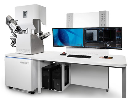
Optimized plasma FIB-SEM platform for high-quality deprocessing of the most modern semiconductor devices with proprietary chemistries • Low-kV high-resolution imaging with enhanced topographic contrast of target layers • Imaging of edges of delayered or cleaved chips using field-free high-resolution technology • Dedicated and proprietary gas chemistries for sub-14 nm nodes deprocessing • End-pointing software module for semiautomated deprocessing enables stopping the process at a desired layer • Electrical characterization of the most sensitive semiconductor devices using in-situ nanoprobing • Easy-to-use, fully customizable, applicationoriented and modular user interface |
About Us|Honor|Products|Contact Us
Copyright ? 京ICP 06010381